
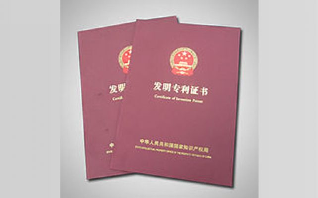
BT Imaging has had another of its key patents for wafer sorting with Photoluminescence Imaging allowed in China (Patent number ZL 201080033122.0).
This brings the total of granted or allowed patents in China to 7 (SEVEN). Another three core patents are hoped to be allowed by the end of 2014.
About BT Imaging
BT Imaging is the leading developer and manufacturer of photoluminescence imaging inspection tools for the photovoltaic industry. Since 2008 when it spun out of the world-renowned University of New South Wales’ School of Photovoltaic and Renewable Energy Engineering, BT Imaging has forged a reputation based on innovation, an extensive patent portfolio, deep research capability, and new product development. BT Imaging’s logo reads ‘Innovate, Control, Yield’ which reflects the company’s vision to provide the manufacturers of photovoltaic wafers, cells and modules with ever-new hardware and software tools that allow unprecedented levels of cost reduction, and increases in production yield and product efficiency. Headquartered in Sydney Australia, privately owned BT Imaging has offices in China, Taiwan and Europe, together with key distributors in Japan, South Korea and the USA.