FOR IMMEDIATE RELEASE
BT IMAGING INTRODUCES BRICK INSPECTION TOOL AND INLINE PL MODULE FOR PROCESSED WAFERS AND CELLS
Sydney, Australia, June 26, 2013 – BT Imaging Pty Ltd. the world’s leading supplier of photoluminescence imaging based inspection and quality control systems for the photovoltaic (PV) manufacturing industry, today announced two new products – the LIS-B1 and the iLS-L2.
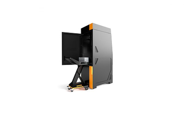
The LIS-B1 is an entirely new product focused solely on the inspection of defects in silicon bricks, the latter cut from silicon blocks or ingots during silicon wafer manufacturing. With the capability of measuring key performance limiting defects in both multi crystalline and mono crystalline silicon bricks, this tool offers enhanced product & process quality control opportunities as well as enabling accelerated and advanced process improvement. Changes to silicon block and ingot manufacturing typically aim at increased revenue via higher throughput, for example by reducing the processing time or by increasing the size of charges for each batch. Such measures have the potential for increasing the likelihood of creating defects that eventually impact on solar cell performance; the new BT Imaging LIS-B1 tool can detect, measure and report these defects in real time with 100% inspection of all sides of every brick in production. The LIS B1 can be configured for manual loading or robot loading subject to customer requirements.
The iLS-L2 is a new Photoluminescence Imaging inspection module for solar cell production lines. It can be deployed at any place in the line after the ‘diffusion’ process step and works for both multi crystalline and mono crystalline wafers and cells. The iLS-W2 inspection module has been designed with an ‘overthe-conveyer-belt’ configuration with minimal eye-safety engineering requirements. The iLS-W2 can be configured with a number of algorithms inclusive of (a) measurement and reporting of solar cellperformance limiting defects in all wafer types (multi-crystalline wafers (normal & high performance) as well as mono-crystalline wafers), and (b) micro-crack detection in mono-crystalline wafers and cells. Additional reporting algorithms are planned to be added to this list as they pass the current beta testing phase.
“We are very proud of these new tools” said Ian Maxwell, CEO, “Our hardware, software and algorithm development teams have been working very closely with trial customers over the last year or so, and these new products have been well received. Our focus has very much been to ensure that we can offer our customers new products that have a very low pay-back period. We would also like to acknowledge the Australian Solar Institute, now part of the Australian Renewable Energy Agency, for assisting with the funding for the product development of these new tools.”
About BT Imaging
BT Imaging designs and builds manufacturing tools used by manufacturers of photovoltaic bricks, wafers and cells. The company is focused on ‘inspection’ manufacturing systems and solutions that are used for quality control, yield enhancement and process control in customer’s factories. The company’s suite of inspection systems combines state-of-the-art hardware and software. BT imaging offers a number of product solutions, many using patented photoluminescence imaging technology; these products help customers increase factory yield and solar cell efficiencies.